Series 1 Version 4, 2 Winding Digital SG CIRCUIT ASSEMBLY
Series 1 Version 5, 2 Winding Digital SG CIRCUIT ASSEMBLY
Second of A Two Winding Digital SG Circuit
What Bedini Basically Knew
Digital Motionless Calculation Tutorial (3 of 3)
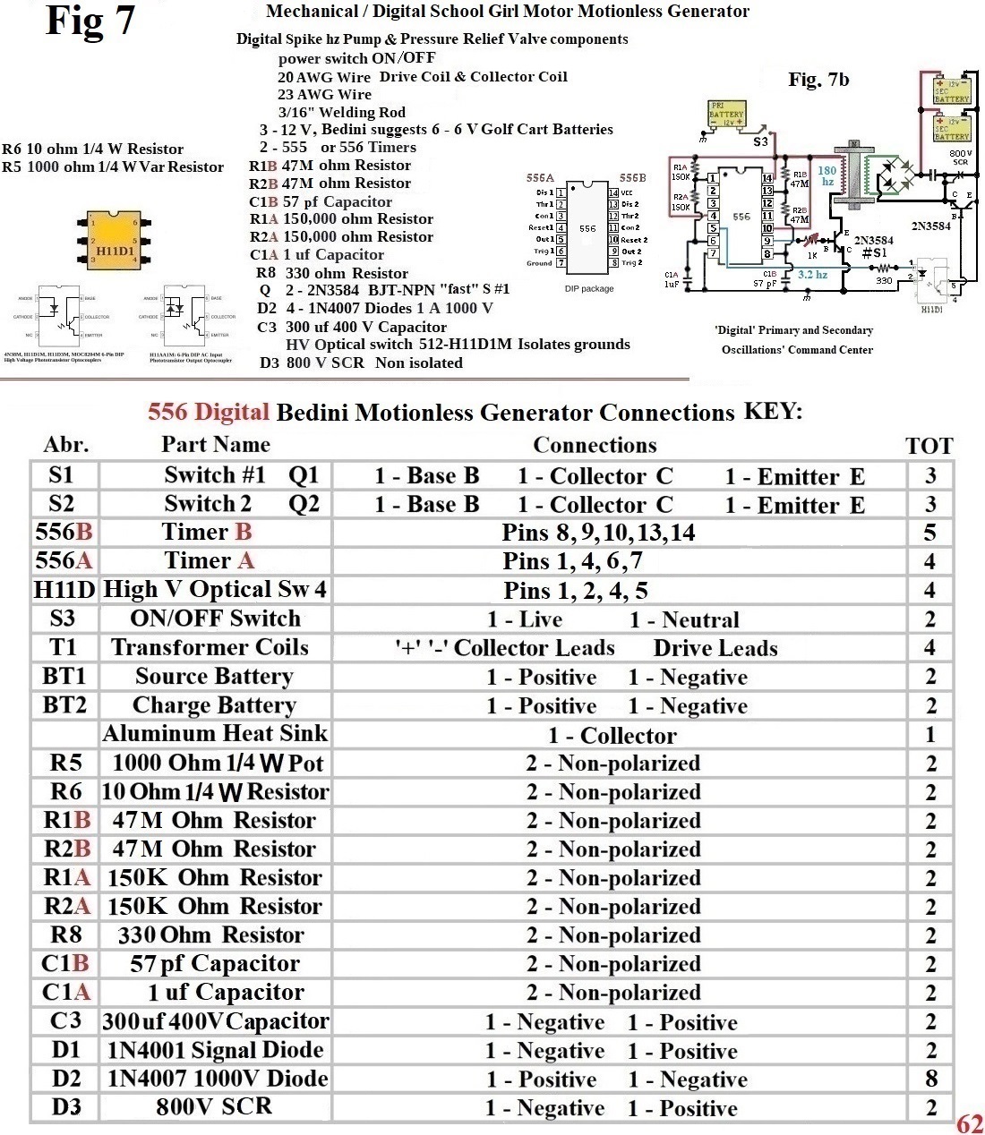
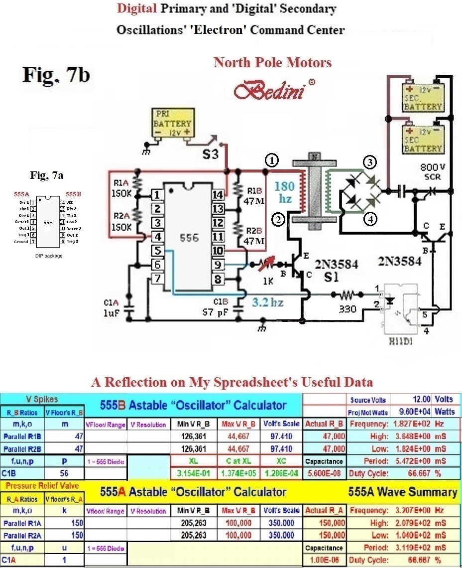
It is of particular Note that neither the components' chart or the schematic above include an R7 between 555B's Pin 3 and the Transistor's Base (or Pin 1). The builder must here recognize that the Transistor Bedini uses for Switch #1 cannot handle more than 7 Volts at the Base. So R7 accommodates the maximum Voltage the Transistor's Base will accept if the Voltage to 555B is greater than 7 Volts.
Assembling Sequence for A Two Winding 556 Digital Primary SG Circuit (3 of 3)
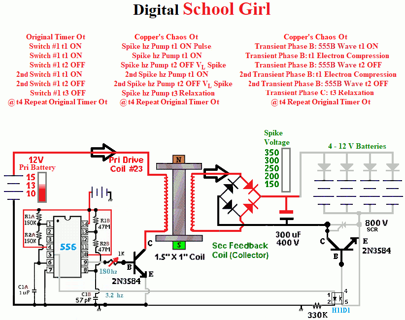
junction
{01} is located at the Drive Coil's North Pole
#23 Wire.
Connect junction
{01}, the Drive
Coil's North Pole #23 Wire, to the
neutral side of S3 (ON/OFF Switch).
Then, also connect another
insulated #26 Wire to the same neutral side of S3 (ON/OFF Switch),
and connect this Wire to 556B's
pin #14
Then, also connect one
lead of R1B (the
first 47 M Timing Resistor) to 556B's
pin #14,
and, after a break,
connect the other end of R1B (the
first 47 M Timing Resistor) to 556B's
pin #13.
Then, also connect R2B
(the second 47 M Timing Resistor) to
556B's pin
#13,
and, after a break, connect the other end of R2B
(the second 47 M Timing Resistor) to
556B's pin
#8.
Then, also connect C1B (the
56 pf Timing Capacitor) to 556B's pin
#8,
and, after a break, connect another insulated #26 Wire to
the other end of C1B (the
56 pf Timing Capacitor),
and connect this Wire to Ground.
Then, after a break, connect another insulated #26 Wire to
556B's pin
#9,
and connect this Wire to Q1's pin #1 (2N3584-2 the Base of
Switch #1),
Then, also connect another insulated #26 Wire to
the same neutral side of S3 (ON/OFF Switch),
and also connect
this Wire to 556A's pin
#4,.
and this Wire also connects to one lead of R1A
(the first 150 K Timing Resistor),
and,
after a break, connect the other end of R1A
(the first 150 K Timing Resistor) to
556A's pin
#1,
Then, also connect one lead of R2A
(the second 150 K Timing Resistor) to
556A's pin
#1,
and, after a break, connect the other end of R2A
(the second 150 K Timing Resistor) to
556A's pin
#6.
Then, also connect C1A (the
1 uf Timing Capacitor) to 556A's
pin #6,
and, after a break, connect another insulated #26 Wire
to the other end of C1A (the
1 uf Timing Capacitor),
and connect this Wire to Ground.
Then,
after a break, connect another insulated #26 Wire to 556A's
pin #5,
and connect this Wire to
R8 (the 330 Resistor),
and, after a break, connect another
insulated #26 Wire to the other side of R8 (the 330 Resistor),
and
connect this Wire to H11D1 pin #1,
and, after a break, connect
another insulated #26 Wire to H11D1 pin #2,
and connect this
Wire to Ground.
junction {02} is located at the
Drive Coil's South Pole #23 Wire.
Connect
junction {02}, the Drive
Coil's South Pole #23 Wire, to Q1's pin
#2 (2N3584-1 the Emitter of Switch #1),
and, after a break,
connect another insulated #23 Wire to Q1's pin #3 (2N3584-1 the
Collector of Switch #1),
and connect this Wire to Ground.
junction {03} is located at the Collector
Coil's North Pole #23 Wire.
Connect
junction {03}, the Collector
Coil's North Pole #23 Wire, to D2's (the
1N4007 4 Diode Bridge) input
and, after a break, connect
another insulated #23 Wire to D2's (the 1N4007 4 Diode Bridge)
positive '+' output,
and also connect this Wire to the positive
'+' lead of C3 (the 300V Capacitor),
and, after a break,
connect another insulated #23 Wire to the negative '-' lead of C3
(the 300V Capacitor),
and connect this Wire to the negative '-'
lead of D3 (the 800V SCR),
and, after a break, connect another
insulated #23 Wire to the positive '+' lead of D3 (the 800V SCR),
and connect this Wire to Q2's pin #2 (2N3584-2 the Emitter of
Switch 2),
and also connect this Wire to H11D1 pin #4,
and,
after a break, connect another insulated #23 Wire to H11D1 pin #5,
and connect this Wire to Q2's pin #1 (2N3584-2 the Base of
Switch 2).
junction {04} is located at the
Collector Coil's South Pole #23 Wire.
Connect junction {04}, the
Collector Coil's South Pole #23 Wire,
to D2's (the 1N4007 4 Diode Bridge) input,
and, after a break,
connect another insulated #23 Wire to D2's (the 1N4007 4 Diode
Bridge) negative '-' output,
and connect this Wire to Q2's pin
#3 (2N3584-2 the Collector of Switch 2).
Either any of my Transient Phase Simulations or the CircuitMaker Program are using Excel
(or Spreadsheet type techniques) for their intense calculations.
It is, therefore, advisable and wise to know Three things:
Any of these resources files can be corrupted if your
computer's resources are over-taxed.
and a requirement to use any of the Transient Phase Simulations is to have Excel or an equivalent.
Preserve Original File, and Work only from a backup to avoid File corruption when using these resources, and be vigilant protecting your work.