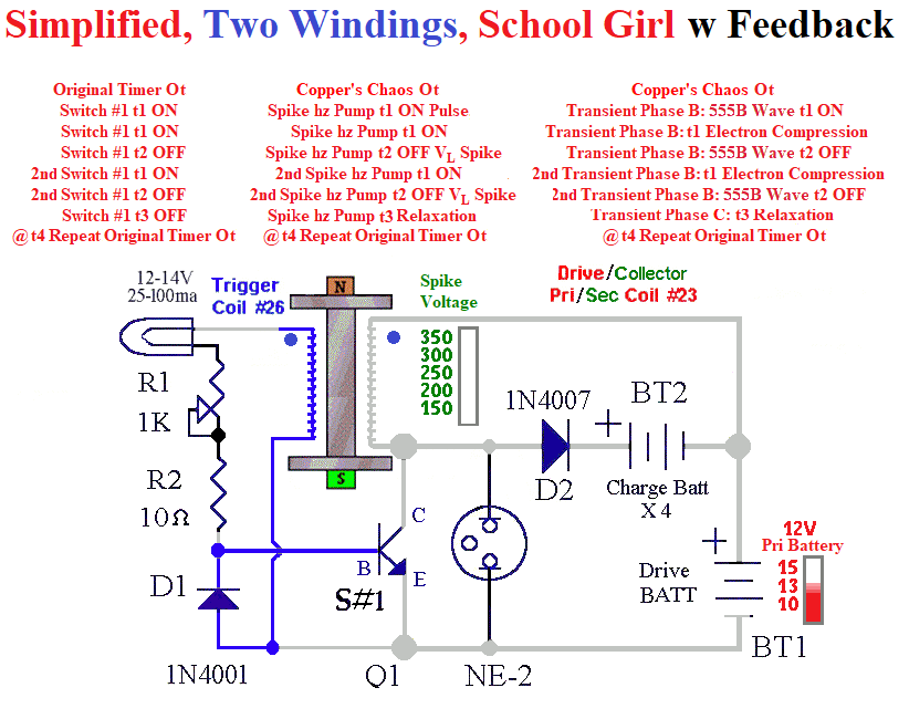
Series 1 Version 7, 2 Winding Digital SG CIRCUIT ASSEMBLY
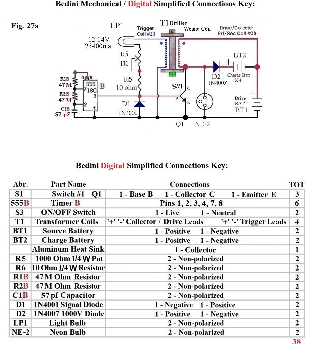
It is of particular Note that neither the components' chart or the schematic above include an R7 between 555B's Pin 3 and the Transistor's Base (or Pin 1). The builder must here recognize that the Transistor Bedini uses for Switch #1 cannot handle more than 7 Volts at the Base. So R7 accommodates the maximum Voltage the Transistor's Base will accept if the Voltage to 555B is greater than 7 Volts.
Analogous Simplified Series 1 Version 8 Circuit Photo
See the Bedini_Monopole (or School Girl) Schematic
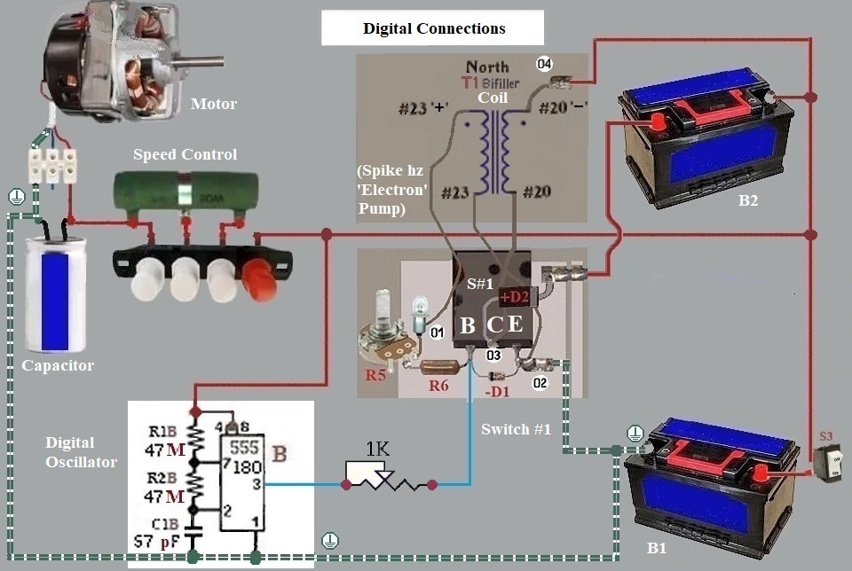
Photo Series 1 Version 8 above corresponds to the Digital Schematic below
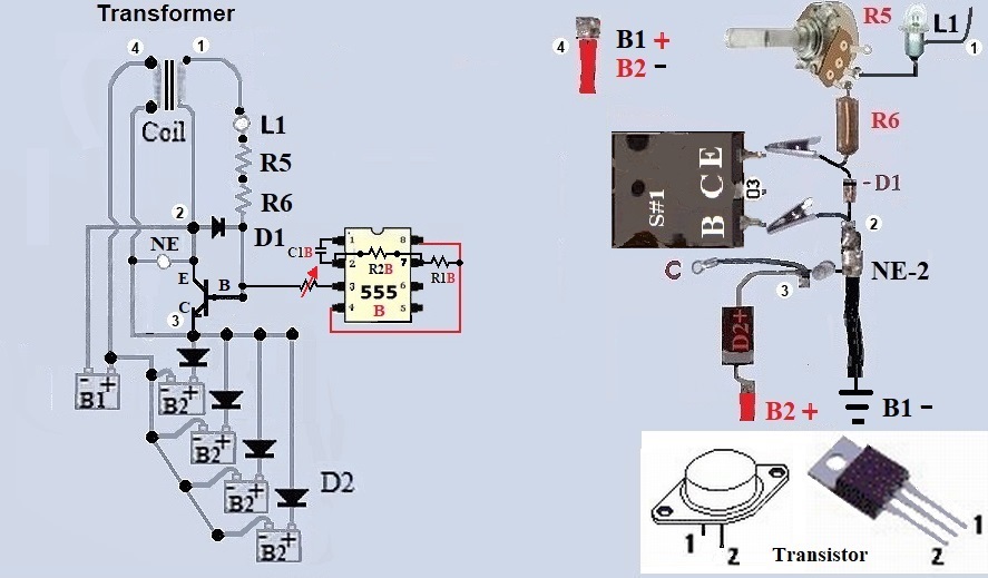
A Simplified Series 1 Version 8 for What Is Now Known Oscillation's Chart
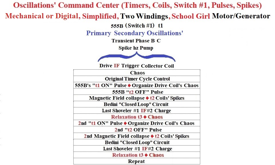
The “Building A Simplified Oscillation's Chart” depicts a general visual for the characteristic design of Bedini's Simplified sequential stages, which can create more Efficient increases in an Electron Density Intensity Energy manifest as Spikes, and still isolate and capture those more Efficient Electron Density Intensity Energy increases.
Assembling
A Simplified Series 1 Version 8
The Two Winding Digital SG Circuit
Instructions
Don't
overheat your Diodes, Resistors, or Transistor when soldering.
John keeps the Wires in his Circuit as short as
possible, going nearly to the quick when fastening his Diodes to the
Transistor. The Energizer Circuit is more Efficient with shorter
Wires (less R).
If you don't know how to solder. use
nuts/bolts to secure your connections.
A 9-V Battery can
be used to verify Circuit functions before soldering the connections
if Alligator clips are used to both connect and hold components in
place until you verify function.
Use heavy gauge Wires
when connecting your Batteries in parallel or series. (less R is
more Efficient).
More on Assembling Series 1 Version 8 of the Simplified SG Schematic
junction
{01} is located at the Trigger Coil's North
Pole #23 Wire
Connect junction
{01}, the Trigger
Coil's North Pole #23 Wire to the
neutral side of S3 (ON/OFF Switch).
Then, also connect another
insulated #23 Wire to the same neutral side of S3 (ON/OFF Switch),
and connect this Wire to LP1,
and, after a break,
connect another Wire to the other end of LP1,
and connect this
Wire to R5 (the 1000 Ohm Pot),
and, after a break, connect the
other end of R5 (the 1000 Ohm Pot) to R6 (the 10 Ohm Resistor),
and, after a break, connect the other end of R6 (the 10 Ohm
Resistor) to Q1's pin #1 (2N3584-1 the Base of Switch #1),
and
also connect D1's negative '-' lead (the 1N4001 Diode) to Q1's pin
#1 (2N3584-1 the Base of Switch #1),
and, after a break,
connect another insulated #23 Wire to D1's positive '+' lead (the
1N4001 Diode),
and connect this Wire to Ground.
junction
{02} is located at the Trigger Coil's South
Pole #23 Wire, and is the BT1's
negative '-' lead (Source Battery or Ground)
Connect junction
{02} the Trigger Coil's South Pole #23 Wire
to another insulated #23 Wire,
and also connect this Wire to
Q1's pin #1 (2N3584-1 the Emitter of Switch #1),
and also
connect this Wire to D1's positive '+' lead (the 1N4001 Diode).
and
also connect this Wire to NE-2.
Then, after a break, connect
an insulated #26 Wire to the same neutral side of S3 (ON/OFF
Switch),
and connect this Wire to 555B's
pin #8
and also connect this Wire
to 555B's pin
#4.
Then, also connect one lead of R1B
(the first 47 M Timing Resistor) to
555B's pin
#4,
and, after a break, connect the other end of R1B
(the first 47 M Timing Resistor) to
555B's pin
#7.
Then, also connect R2B (the
second 47 M Timing Resistor) to 555B's
pin #7,
and, after a break, connect the other end of R2B
(the second 47 M Timing Resistor) to
555B's pin
#2,
and, also connect C1B (the
56 pf Timing Capacitor) to 555B's pin
#2,
and, after a break, connect the other end of C1B
(the 56 pf Timing Capacitor) to 555B's
pin #1,
and also connect another
insulated #26 Wire to 555B's pin
#1,
and connect this Wire to Ground.
Then, after a
break, connect an insulated #26 Wire to 555B's
pin #3,
and connect this #26 Wire
to Q1's pin #1 (2N3584-1 the Base of Switch #1),
and, after a
break, connect another insulated #26 Wire to the other side of R7
(the 330 Resistor),
and connect this Wire to H11D1 pin #1,
and, after a break, connect another insulated #26 Wire to
H11D1 pin #2,
and connect this Wire to Ground.
junction
{03} is located at the Drive/Collector Coil's
South Pole #20 Wire
Connect
junction {03}, the Drive/Collector
Coil's South Pole #20 Wire to an
insulated #20 Wire,
and also connect this Wire to NE-2,
and
also connect this Wire to a D2's '+' (the 1N4007 Diode's positive
'+' lead),
and, after a break, connect D2's negative '-' lead
(the 1N4007 Diode) to BT2's positive '+' lead (the Charge Battery).
junction
{04} is located at the
Drive/Collector Coil's North Pole #20 Wire
Connect
junction {04}, the Drive/Collector
Coil's North Pole #20 Wire to an
insulated #20 Wire,
and connect this Wire to BT2's negative
'-' lead (the Charge Battery),
and also the neutral side of S3
(the ON/OFF switch),
and, after a break, connect another
insulated #20 Wire to the live side of S3 (the ON/OFF switch),
and
connect this Wire to BT1's positive '+' lead (the Source Battery),
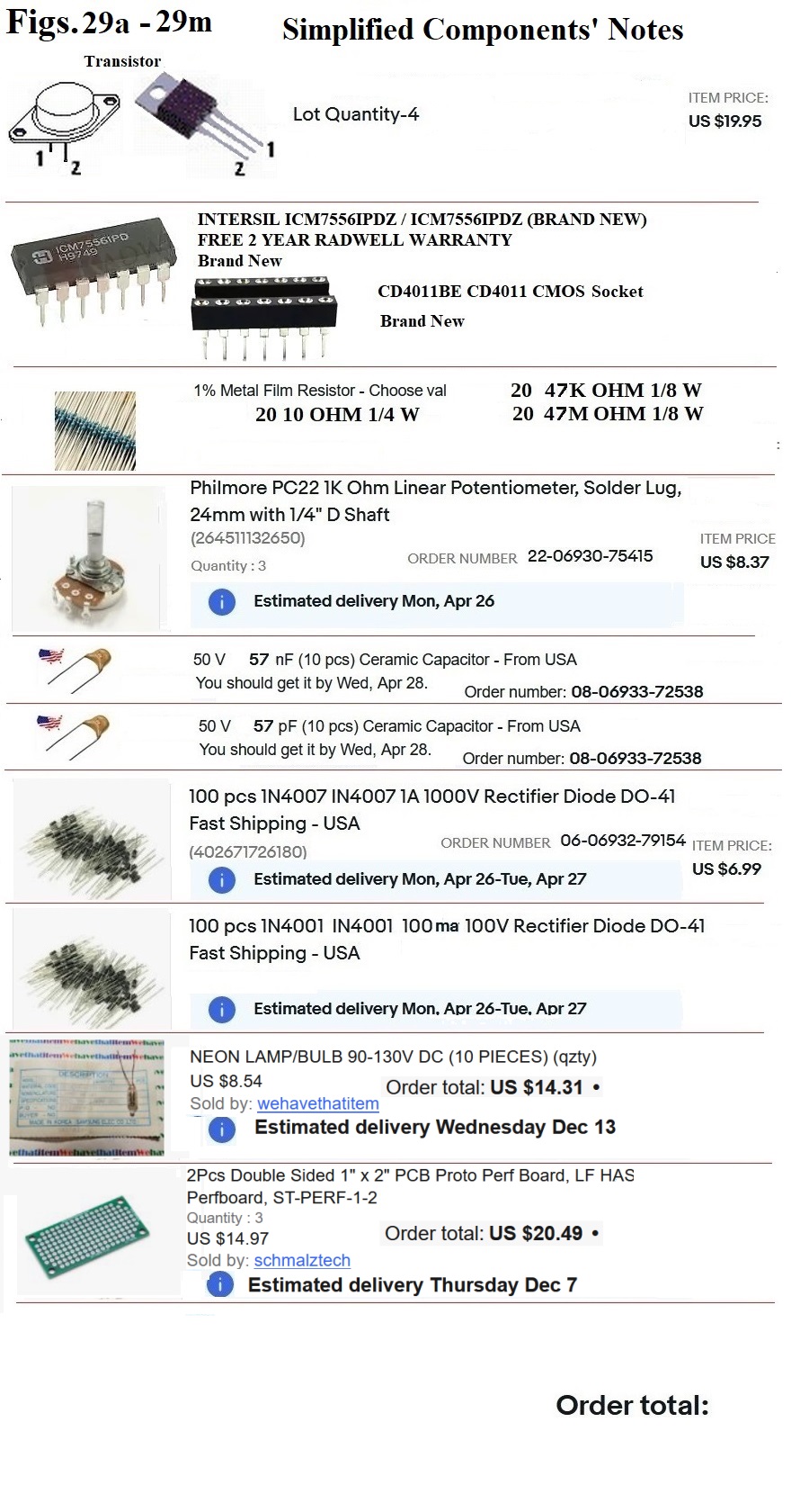
Copper
Winding Wires
Aluminum Heat Sink
Either any of my Transient Phase Simulations or the CircuitMaker Program are using Excel
(or Spreadsheet type techniques) for their intense calculations.
It is, therefore, advisable and wise to know Three things:
Any of these resources files can be corrupted if your
computer's resources are over-taxed.
and a requirement to use any of the Transient Phase Simulations is to have Excel or an equivalent.
Preserve Original File, and Work only from a backup to avoid File corruption when using these resources, and be vigilant protecting your work.