eternaltruth.net

What Bedini Knew of Tesla

Copyright© 2008, E C Distributions


Build What Bedini Knew

Three events occur in the Coils during a Spike hz Electron Pump's Transient t2 Phase C when a Switch #1's “t2 OFF” Impulse influences an Electric and Magnetic Field. A large VL Spike may be created by the Reluctance of the Inductive Reactance (or Inductance), where the magnitude of the collapsing Electric and Magnetic Field is partially dependent on Switch #1's "t2 OFF" Timing, and the Impulse's expanding and collapsing Electric and Magnetic Field is allowed to return its accumulated non-Ghosted Electron Energy, that has become greater than its Source V, to the Coils. This isolated Current's Impulse Density Intensity Field, caused by Switch #1's “t2 OFF,” has been amplified by an Impulse's VL Spike's non-Ghosted Electrons and then captured within the Transient Phase.

These t1 and t2 Timing series' cycles (Transient Phases B and C from Fig. 23) of Switch #1's "t1 ON," in concert with the "shorted Coil's Electron building Transient t1 Phase B until the Electron Energy compressed equals the target AVE DC," and Switch #1's "t2 OFF", (or Transient t2 Phase C), is creating a VL Spike along with Transient t2 Phase's secondary t1, introduced through the 1K tuning Resistor, follows with another t2's expanding and collapsing Magnetic Field, and this series and cycle ends with Transient t3's Relaxation Phase. (The secondary t1 and t2 are simply doubling the Mechanical version's VL Spike's frequency to increase the AVE DC.)

All these Impulse events transpire in
a symphony of Magnetic Fields, which both split the positives and capture all the Transient Phases' Electric and Magnetic Fields' FREE Electron expansions and collapses throughout each series of the cyclic process, reaching beyond "Zero Point Energy." Each Transient Phases Coils' series encapsulates the innate Electron response and Efficiency of Tesla's design, and prepares Tinkerers for What We Now Know Beyond Bedini Generators.


School Girl Oscillation's Chart

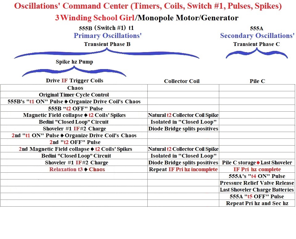
The “School Girl Oscillation's Chart” depicts a general visual for the characteristic design of Bedini's sequential stages, which create an increase in Electron Density Intensity Energy manifest as a Spike, and then isolate and capture that Electron Density Intensity Energy increase.


A Mechanical Three Winding SG Circuit

555 Timer Calculations

What Bedini Basically Knew

A Mechanical Three Winding SG Circuit Calculation Tutorial (1 of 3)

It is of particular Note that neither the components' chart or the Mechanical schematic above include an R7 between 555B's Pin 3 and the Transistor's Base (or Pin 1). The builder must here recognize that the Transistor Bedini uses for Switch #1 cannot handle more than 7 Volts at the Base. So R7 accommodates the maximum Voltage the Transistor's Base will accept if the Voltage to 555B is greater than 7 Volts The Mechanical version does not generate more than 7 Volts and, therefore, does mot require an R7.


Assembling Sequence for A Mechanical Three Winding SG Circuit (1 of 3)

junction {01} is located at the Drive Coil's North Pole #23 Wire.
Connect
junction {01}, the Drive Coil's North Pole #23 Wire, to the neutral side of S3 (ON/OFF Switch).
Then, also connect another insulated #26 Wire to the same neutral side of S3 (ON/OFF Switch),
and connect this Wire to 555
A's pin #8
and also connect this Wire to 555
A's pin #4.
Then, also connect one lead of R1
A (the first 150 K Timing Resistor) to 555A's pin #4,
and, after a break, connect the other end of R1
A (the first 150 K Timing Resistor) to 555A's pin #7.
Then, also connect R2
A (the second 150 K Timing Resistor) to 555A's pin #7,
and, after a break, connect the other end of R2
A (the second 150 K Timing Resistor) to 555A's pin #2.
Then, also connect C1
A (the 1 uf Timing Capacitor) to 555A's pin #2,
and, after a break, connect the other end of C1
A (the 1 uf Timing Capacitor) to 555A's pin #1,
and, then, also connect another insulated #26 Wire to 555
A's pin #1,
and connect this Wire to Ground.
Then, after a break, connect another insulated #26 Wire to 555
A's pin #3,
and connect this Wire to R8 (the 330 Resistor),
and, after a break, connect another insulated #26 Wire to the other side of R8 (the 330 Resistor),
and connect this Wire to H11D1 pin #1,
and, after a break, connect another insulated #26 Wire to H11D1 pin #2,
and connect this Wire to Ground.
junction {02} is located at the Drive Coil's South Pole #23 Wire.
Connect
junction {02}, the Drive Coil's South Pole #23 Wire, to Q1's pin #2 (2N3584-1 the Emitter of Switch #1),
and, after a break, connect another insulated #23 Wire to Q1's pin #3 (2N3584-1 the Collector of Switch #1),
and connect this Wire to Ground.

junction {03} is located at the Collector Coil's North Pole #23 Wire.
Connect
junction {03}, the Collector Coil's North Pole #23 Wire, to D2's (the 1N4007 4 Diode Bridge) input
and, after a break, connect another insulated #23 Wire to D2's (the 1N4007 4 Diode Bridge) positive '+' output,
and also connect this Wire to the positive '+' lead of C3 (the 300V Capacitor),
and, after a break, connect another insulated #23 Wire to the negative '-' lead of C3 (the 300V Capacitor),
and connect this Wire to the negative '-' lead of D3 (the 800V SCR),
and, after a break, connect another insulated #23 Wire to the positive '+' lead of D3 (the 800V SCR),
and connect this Wire to Q2's pin #2 (2N3584-2 the Emitter of Switch 2),
and also connect this Wire to H11D1 pin #4,
and, after a break, connect another insulated #23 Wire to H11D1 pin #5,
and connect this Wire to Q2's pin #1 (2N3584-2 the Base of Switch 2).

junction {04} is located at the Collector Coil's South Pole #23 Wire.
Connect
junction {04}, the Collector Coil's South Pole #23 Wire, to D2's (the 1N4007 4 Diode Bridge) input,
and, after a break, connect another insulated #23 Wire to D2's (the 1N4007 4 Diode Bridge) negative '-' output,
and connect this Wire to Q2's pin #3 (2N3584-2 the Collector of Switch 2).

junction {05} is located at the Trigger Coil's North Pole #26 Wire.
Connect
junction {05}, the Trigger Coil's North Pole #26 Wire, to LP1,
and, after a break, connect another insulated #26 Wire to the other end of LP1,
and connect this Wire to R5 (the 1000 Ohm Pot),
and, after a break, connect another insulated #26 Wire to the other end of R5 (the 1000 Ohm Pot),
and connect this Wire to R6 (the 10 Ohm Resistor),
and, after a break, connect another insulated #26 Wire to the other end of R6 (the 10 Ohm Resistor),
and connect this Wire to to Q1's pin #1 (2N3584-2 the Base of Switch #1),
and also connect this Wire to D1's (the 1N4001 Diode) negative '-' lead,
and, after a break, connect another insulated #26 Wire to D1's (the 1N4001 Diode) positive '+' lead,
and connect this Wire to Ground.

junction {06} is located at the Trigger Coil's South Pole #26 Wire.
Connect
junction {06}, the Trigger Coil's South Pole #26 Wire, to Ground.


First of A Two Winding Digital SG Circuit

555 Timer Calculations

What Bedini Basically Knew

Digital Calculation Tutorial (2 of 3)


It is of particular Note that neither the components' chart or the schematic above include an R7 between 555B's Pin 3 and the Transistor's Base (or Pin 1). The builder must here recognize that the Transistor Bedini uses for Switch #1 cannot handle more than 7 Volts at the Base. So R7 accommodates the maximum Voltage the Transistor's Base will accept if the Voltage to 555B is greater than 7 Volts.


Assembling Sequence for A Two Winding 555 or a 556 Digital Primary SG Circuit (2 of 3)

junction {01} is located at the Drive Coil's North Pole #23 Wire.
Connect
junction {01}, the Drive Coil's North Pole #23 Wire, to the neutral side of S3 (ON/OFF Switch).
Then, also connect another insulated #26 Wire to the same neutral side of S3 (ON/OFF Switch),
and connect this Wire to 555
B's pin #8
and also connect this Wire to 555
B's pin #4.
Then, also connect one lead of R1
B (the first 47 K Timing Resistor) to 555B's pin #4,
and, after a break, connect the other end of R1
B (the first 47 K Timing Resistor) to 555B's pin #7.
Then, also connect R2
B (the second 47 K Timing Resistor) to 555B's pin #7,
and, after a break, connect the other end of R2
B (the second 47 K Timing Resistor) to 555B's pin #2.
Then, also connect C1
B (the 56 nf Timing Capacitor) to 555B's pin #2,
and, after a break, connect the other end of C1
B (the 56 nf Timing Capacitor) to 555B's pin #1,
and, then, also connect another insulated #26 Wire to 555
B's pin #1,
and connect this Wire to Ground.
Then, after a break, connect another insulated #26 Wire to 555
B's pin #3,
and connect this Wire to Q1's pin #1 (2N3584-2 the Base of Switch #1),
Then, also connect another insulated #26 Wire to the same neutral side of S3 (ON/OFF Switch),
and connect this Wire to 555
A's pin #8
and also connect this Wire to 555
A's pin #4.
Then, also connect one lead of R1
A (the first 150 K Timing Resistor) to 555A's pin #4,
and, after a break, connect the other end of R1
A (the first 150 K Timing Resistor) to 555A's pin #7.
Then, also connect R2
A (the second 150 K Timing Resistor) to 555A's pin #7,
and, after a break, connect the other end of R2
A (the second 150 K Timing Resistor) to 555A's pin #2.
Then, also connect C1
A (the 1 uf Timing Capacitor) to 555A's pin #2,
and, after a break, connect the other end of C1
A (the 1 uf Timing Capacitor) to 555A's pin #1,
and, then, also connect another insulated #26 Wire to 555
A's pin #1,
and connect this Wire to Ground.
Then, after a break, connect another insulated #26 Wire to 555
A's pin #3,
and connect this Wire to R8 (the 330 Resistor),
and, after a break, connect another insulated #26 Wire to the other side of R8 (the 330 Resistor),
and connect this Wire to H11D1 pin #1,
and, after a break, connect another insulated #26 Wire to H11D1 pin #2,
and connect this Wire to Ground.

junction {02} is located at the Drive Coil's South Pole #23 Wire.
Connect
junction {02}, the Drive Coil's South Pole #23 Wire, to Q1's pin #2 (2N3584-1 the Emitter of Switch #1),
and, after a break, connect another insulated #23 Wire to Q1's pin #3 (2N3584-1 the Collector of Switch #1),
and connect this Wire to Ground.

junction {03} is located at the Collector Coil's North Pole #23 Wire.
Connect
junction {03}, the Collector Coil's North Pole #23 Wire, to D2's (the 1N4007 4 Diode Bridge) input
and, after a break, connect another insulated #23 Wire to D2's (the 1N4007 4 Diode Bridge) positive '+' output,
and also connect this Wire to the positive '+' lead of C3 (the 300V Capacitor),
and, after a break, connect another insulated #23 Wire to the negative '-' lead of C3 (the 300V Capacitor),
and connect this Wire to the negative '-' lead of D3 (the 800V SCR),
and, after a break, connect another insulated #23 Wire to the positive '+' lead of D3 (the 800V SCR),
and connect this Wire to Q2's pin #2 (2N3584-2 the Emitter of Switch 2),
and also connect this Wire to H11D1 pin #4,
and, after a break, connect another insulated #23 Wire to H11D1 pin #5,
and connect this Wire to Q2's pin #1 (2N3584-2 the Base of Switch 2).

junction {04} is located at the Collector Coil's South Pole #23 Wire.
Connect
junction {04}, the Collector Coil's South Pole #23 Wire, to D2's (the 1N4007 4 Diode Bridge) input,
and, after a break, connect another insulated #23 Wire to D2's (the 1N4007 4 Diode Bridge) negative '-' output,
and connect this Wire to Q2's pin #3 (2N3584-2 the Collector of Switch 2).


Second of A Two Winding Digital SG Circuit

555 Timer Calculations

What Bedini Basically Knew

Digital Motionless Calculation Tutorial (3 of 3)


It is of particular Note that neither the components' chart or the schematic above include an R7 between 555B's Pin 3 and the Transistor's Base (or Pin 1). The builder must here recognize that the Transistor Bedini uses for Switch #1 cannot handle more than 7 Volts at the Base. So R7 accommodates the maximum Voltage the Transistor's Base will accept if the Voltage to 555B is greater than 7 Volts.


Assembling Sequence for A Two Winding 556 Digital Primary SG Circuit (3 of 3)

junction {01} is located at the Drive Coil's North Pole #23 Wire.
Connect
junction {01}, the Drive Coil's North Pole #23 Wire, to the neutral side of S3 (ON/OFF Switch).
Then, also connect another insulated #26 Wire to the same neutral side of S3 (ON/OFF Switch),
and connect this Wire to 556
B's pin #14
Then, also connect one lead of R1
B (the first 47 M Timing Resistor) to 556B's pin #14,
and, after a break, connect the other end of R1
B (the first 47 M Timing Resistor) to 556B's pin #13.
Then, also connect R2
B (the second 47 M Timing Resistor) to 556B's pin #13,
and, after a break, connect the other end of R2
B (the second 47 M Timing Resistor) to 556B's pin #8.
Then, also connect C1
B (the 56 pf Timing Capacitor) to 556B's pin #8,
and, after a break, connect another insulated #26 Wire to the other end of C1
B (the 56 pf Timing Capacitor),
and connect this Wire to Ground.
Then, after a break, connect another insulated #26 Wire to 556
B's pin #9,
and connect this Wire to Q1's pin #1 (2N3584-2 the Base of Switch #1),
Then, also connect another insulated #26 Wire to the same neutral side of S3 (ON/OFF Switch),
and also connect this Wire to 556
A's pin #4,.
and this Wire also connects to one lead of R1
A (the first 150 K Timing Resistor),
and, after a break, connect the other end of R1
A (the first 150 K Timing Resistor) to 556A's pin #1,
Then, also connect one lead of R2
A (the second 150 K Timing Resistor) to 556A's pin #1,
and, after a break, connect the other end of R2
A (the second 150 K Timing Resistor) to 556A's pin #6.
Then, also connect C1
A (the 1 uf Timing Capacitor) to 556A's pin #6,
and, after a break, connect another insulated #26 Wire to the other end of C1
A (the 1 uf Timing Capacitor),
and connect this Wire to Ground.
Then, after a break, connect another insulated #26 Wire to 556
A's pin #5,
and connect this Wire to R8 (the 330 Resistor),
and, after a break, connect another insulated #26 Wire to the other side of R8 (the 330 Resistor),
and connect this Wire to H11D1 pin #1,
and, after a break, connect another insulated #26 Wire to H11D1 pin #2,
and connect this Wire to Ground.

junction {02} is located at the Drive Coil's South Pole #23 Wire.
Connect
junction {02}, the Drive Coil's South Pole #23 Wire, to Q1's pin #2 (2N3584-1 the Emitter of Switch #1),
and, after a break, connect another insulated #23 Wire to Q1's pin #3 (2N3584-1 the Collector of Switch #1),
and connect this Wire to Ground.

junction {03} is located at the Collector Coil's North Pole #23 Wire.
Connect
junction {03}, the Collector Coil's North Pole #23 Wire, to D2's (the 1N4007 4 Diode Bridge) input
and, after a break, connect another insulated #23 Wire to D2's (the 1N4007 4 Diode Bridge) positive '+' output,
and also connect this Wire to the positive '+' lead of C3 (the 300V Capacitor),
and, after a break, connect another insulated #23 Wire to the negative '-' lead of C3 (the 300V Capacitor),
and connect this Wire to the negative '-' lead of D3 (the 800V SCR),
and, after a break, connect another insulated #23 Wire to the positive '+' lead of D3 (the 800V SCR),
and connect this Wire to Q2's pin #2 (2N3584-2 the Emitter of Switch 2),
and also connect this Wire to H11D1 pin #4,
and, after a break, connect another insulated #23 Wire to H11D1 pin #5,
and connect this Wire to Q2's pin #1 (2N3584-2 the Base of Switch 2).

junction {04} is located at the Collector Coil's South Pole #23 Wire.
Connect
junction {04}, the Collector Coil's South Pole #23 Wire, to D2's (the 1N4007 4 Diode Bridge) input,
and, after a break, connect another insulated #23 Wire to D2's (the 1N4007 4 Diode Bridge) negative '-' output,
and connect this Wire to Q2's pin #3 (2N3584-2 the Collector of Switch 2).


The Simulation requires Excel, or an equivalent.
Preserve Original File,
this Transient Phase Simulation's File can be corrupted
if your computer's resources are over-taxed.
Work only from a backup to avoid File corruption


Return Home